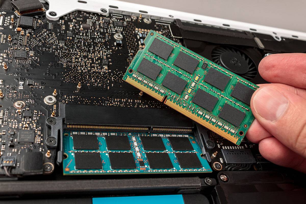
The miniaturization revolution has swept across the globe, transforming industries and shaping the future of electronics. From sleek smartphones and wearables to intricate medical devices and powerful industrial controllers, the demand for smaller, more powerful PCBs is undeniable. However achieving successful miniaturization requires meticulous planning, strategic component selection, and a deep understanding of global design and manufacturing considerations. This article delves into the intricacies of miniaturized PCB design, offering valuable insights and practical tips for navigating the complexities of the international market.
Understanding the Global Miniaturization Landscape
The miniaturization trend is fueled by several key forces
- Exponential growth of portable electronics: Consumers worldwide crave smartphones, tablets, and wearables that are thin, light, and packed with features.
- Space constraints in diverse applications: As devices shrink across industries, from medical implants to industrial controllers, so does the available space for internal components. Miniaturization helps pack more functionality into smaller form factors.
- Advancements in microelectronics: Smaller, more powerful components like microcontrollers and sensors are constantly emerging, paving the way for highly miniaturized designs.
- Internet of Things (IoT) boom: The ever-expanding IoT landscape necessitates miniaturization for resource-constrained sensors and connected devices across various sectors.
Benefits of Miniaturized PCBs on a Global Scale
Miniaturization offers numerous advantages for manufacturers and consumers alike
- Reduced weight and size: This is crucial for portable devices, enhancing user experience and portability across various cultures and preferences.
- Enhanced functionality: Smaller boards can accommodate more components, leading to feature-rich devices with advanced capabilities for diverse applications.
- Improved power efficiency: Smaller boards often require less power, extending battery life for devices used on the go, regardless of location.
- Cost-effectiveness: Efficient material utilization and streamlined manufacturing processes can potentially reduce production costs, impacting global markets positively.
PCB Design Tips for Global Miniaturization Success
Component Selection
- Embrace high-density components: Opt for smaller footprints like 0201, 0402, or even 01005 packages, considering their global availability and cost-effectiveness.
- Explore integration: Utilize multichip modules (MCMs) or system-in-package (SiP) solutions to consolidate components onto a single substrate, reducing board size and complexity.
- Prioritize passive component miniaturization: Utilize chip resistors, chip capacitors, and inductors with small footprints. Consider leadless (SMT) or molded options for space savings.
Board Layout Optimization
- Master the art of trace routing: Employ techniques like minimizing trace length, using stacked vias, and carefully considering signal integrity, especially for high-speed designs.
- Strategize component placement: Carefully place components to minimize board size and signal path lengths while paying close attention to thermal management, especially for heat-generating components.
- Embrace multi-layer boards: Utilize multiple layers for complex designs, but carefully evaluate cost implications based on global manufacturing capabilities and market demands.
Material Selection
- Consider advanced substrates: Explore high-density interconnect (HDI) materials like BT, LCP, or coreless prepreg for extreme miniaturization.
- Unlock the potential of flex circuits: For space-constrained applications or three-dimensional designs, consider flexible PCBs, but be mindful of their cost and design complexities.
Manufacturing Considerations
- Fine-line printing: Employ narrower trace widths and spacings, but ensure manufacturability based on your chosen PCB manufacturer’s capabilities and global industry standards.
- Leverage microvias: Utilize microvias for signal routing through inner layers, but be mindful of drilling costs and potential yield issues.
- Explore advanced assembly techniques: Consider techniques like flip-chip or ball grid array (BGA) for high-density component placement, but evaluate their cost-effectiveness and global feasibility.
Additional Considerations for the Global Market
- Regulatory compliance: Ensure your miniaturized designs adhere to relevant safety and environmental regulations across your target markets.
- Global supply chain management: Secure reliable and cost-effective component suppliers with a global presence to avoid disruptions.
- Design for manufacturability (DFM): Partner with experienced PCB manufacturers early in the design process to ensure global manufacturability and cost optimization.
- Thermal management: Carefully consider heat dissipation strategies, especially for miniaturized designs, to ensure global reliability under diverse environmental conditions.
References
1. IPC (Institute for Printed Circuits)
Stay tuned for more expert tips and industry insights on PCB design and miniaturization trends. Discover how to navigate the complexities of shrinking PCBs while optimizing performance for a global market.

